 |
 |
 |
 |
 |
|
 |
|
By Madis Lobjakas, Stephan Zegherd & Janus Krarup
Background Debugging Mode is a special feature of Motorola 683xx MCU's. It allows you to interface to the MCU and perform various operations. The usefull things that can be done from here are reading, writing memory (including memory mapped I/O) and single-stepping through code. Programs can be uploaded into RAM and executed from there. To access this mode, you need a simple interface and a special terminal program running on a PC. What does this have to do with Motorola GSM phones? Every single Motorola GSM phone until (and with) the 8400 used the MC68332. The next generation consisting of the 8700/d460 until the cd920/d520 used the MC68338. The very latest units like the v and m series does not use a Motorola MCU and hence has no BDM capabilities. To use this special MCU feature, you WILL have to open your phone and do some soldering. Here is what you need to get started:
1. First You need a IBM-PC compatible computer with free LPT (printer) port. Even old slow XT is OK.
2. Download software. I recommend BD32 debuger by Scott Howard. This is an exellent tool with built-in simple macro language and and disassembler. And it is freeware.
3. Now You have to build small piece of hardware circuit diagram can be found in downloaded archive bd32-122.zip - copy file "bdm-if.prn" directly into Epson compatible printer to get needed scheme. Or look at aplication note #1230 from Motorola. Another nice diagram is available here.
The shopping list is short:
1 74HC76
2 74HC132
3. resistor 10kOhm
4. capacitor 0.1uF
5. capacitor 0.01uF
6. D25Male connector
7. Diode generic Si Low power (1N4148 for example)
8. Piece of protoype board and less than 0.5m of montage wire
9. 8 or 10 pin (2x4 or 2x5 0.1") header
If 74HC76 is difficult to find then it can be replaced by
more common 74HC74 and then circuit diagram can be found on other
great page. All the components are generic and
cheap. I spent less than 2 EUR for all the above stuff.
It's also possible to substitute the 74132 with a 7474 and a 7414
propely connected by just know very basic TTL logic laws. The
most important thing is that, as the circuit could be powered by
a nominal voltage less than 5V, CMOS TTL logics are required.
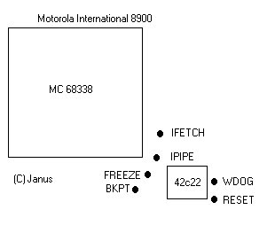
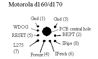
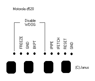
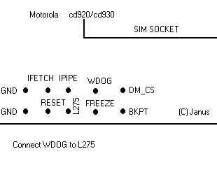
4. It's time to open the phone. The 8900, StarTac130,
d160/170, d520 and cd920/930 are good phones because they have
very easy accesable BDM connection pads: all cd930/920 I
have seen have even clear markings for all pads.
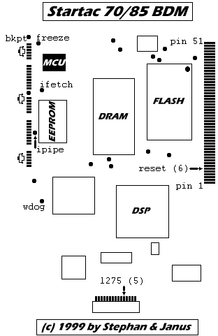
StarTac 70/85 have offcourse some easily accesable pads, but
requires some skills when soldering reset to the big service
connector at the right of the PCB: the rest is easy.
Other older phones have big enough MCU's and BDM wires can be soldered directly to MCU pins. I will work equally well, but requires a steady hand. The pins you need to access are clustered together. I have sucessfully used BDM on an 8200 in this way.
The GSM phones have a software watchdog that we will have to disable in order to make it easier to work with BDM. A watchdog is a feature of the MCU that is used to check if the program executes as intended and doesn't enter a loop that it can't exit from. The program running on the phone will have to reset a status flag with regular intervals or the watchdog will reset the MCU. If 500 miliseconds goes by without the MCU resetting the watchdog, the watchdog will assume that the program has crashed. The hardware watchdog that is part of the power controller (CAR on older phones) will then power down the phone. When entering BDM mode and halting the MCU, the watchdog will think the program crashed and the hardware watchdog will power down the phone as soon as normal operation is resumed. The hardware watchdog can be disabled manually, by connecting "WD" or "WDOG" pad to high logic level (power pad labeled "L275" ).In this way, you can resume MCU operation and continue the execution o fthe program when returning from the halted state (It is not enough to disable the software watchdog through the appropriate MCU register.)
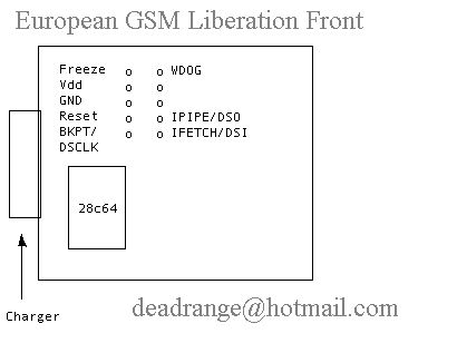
Other wires are exactly like on interface circuit diagram
so here are some layouts:
|
|
|
|
| |
|
| |
|
5. Read the document "bd32.doc" to configure interface. Configuration information is stored in "bd32.cfg". Frist line is the name of the port that the interface is plugged into. The second line contains the delay parameter that is depandable of the speed of your computer (0 for XT and >130 for fast pentium).
| Here are some guidelines for the speed setting: P-266 : 290 |
6. First test: Run bd32.exe and turn phone on. Issue command "reset". Does phone restart? If phone simply turns off then "WD" pin has no constant high voltage. If nothing happens check your interface hardware and cibbectir wiring once more.
7. If reset was sucsessful, then the msetup is working and you can start to use it. In windowed mode, it will look like this:
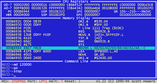
The basic commands that you should know about are: md (memory dump) and mm (memory modify).
The memory map if the motorola phones are very conserved from model to model. The basic layout is like this:
0x000000-0x003FFF Boot loader
0x004000-0x0FFFFF Main program
0x100000-0x11FFFF RAM
0x120000-0x121FFF EEPROM
The memory map can always be derived by following program
execution from reset and studying the chip select registers. RAM
can be read and written, FLASH is read-only and EEPROM can be
both read and written. However before the EEPROM can be written
to, the WE line has to be activated through ChipSelectOption5
(FFFA62). It must be changed from 48F0 to 58F0: (in one case, you
just set bit 0 of the first nibble).
mm 0xfffa62 <CR>
0x58f0 <CR>
After this step, you can wirite to the EEPROM. Some units have
the AT28C64B which incorporates software data protection (SDP).
SDP is disabled by a write sequence as follows:
mm 0x121554, 00AA.
mm 0x120AAA, 5500.
mm 0x121554, 00A0.
This according to datasheet.
Other interesting things to map are the I/O ports. For example try 0xFFFA19 on the cd9x0 and StarTAC 85, bits 0-2 are the vibrator, green and red LED's. The MC68332 / MC68338 manual is your friend and an absolute must for this work.
The BDM-v090 program has been modified (By Madis and TST) to support the Intel flash ROM used in the recent Motorola phones like the cd9x0, d160 and d520. The original source is available from Motorola. This means that with the simple program, you can backup and restore the Flash ROM, EEPROM and RAM - depending on the computer speed, flashing the ROM can take up to 30 mins, but a pentium should typically do it in 12 mins. After specifying the LPT: port used and the port speed, the folowing options are available:
| Reset Target MCU to enable BDM! (R /
K ) Enter Command BDCEFHIMRSQWZ('H' for Help):h Help for BDMFLASH: R: Hardware Reset Target MCU K: Init Phone B: Begin Program Execution from Reset S: Single Step Target MCU G: Start Programm Execution from Address D: Dump Target MCU Registers M: Memory Hex/ASCII Display W: Write memory bytewise (not working properly yet) L: Load S-Record File into Target I: Get Flash ROM Man.ID and Dev. ID C: Clean one Block of Flash ROM E: Write binary file to EEPROM F: Write binary file to Flash ROM X: Write binary file to RAM Z: Dump Target to binary file H: Print This Help Summary Q: Quit back to DOS |
Remember that all numbers are in HEX. Please note that also this program in not intended to be used by the casual user that think to start playing with these things without a prior discrete background of the inner workings of how CPU32 works and/or various devices connected to it: you and only you are responsabile of your actions.
With this program and the BDM interface, you have the tools for upgrading the firmware of your motorola phone (if you are not afraid to open it and solder). First of all, make a complete backup of your phone (Dump ROM from 0x000000, length 0x100000, EEPROM from 0x120000, length 0x2000 and MCURAM from 0xFFFA00, length 0x80) and keep those files in a safe place! Afterwards it's impossible to damage your phone except with physical effort, because you can restore the MCU configuration and flash the data back any time via BDM.
BD32 can execute macros and target resident programs can be used to make many tasks a lot faster - especially if the BDM interface bandwith becomes limiting. Madis made a range of macros for the Motorola d160, allowing you to write to EEPROM / FLASH and dump memory to disk. If you are planning to *really* play with your phone, then you can find some really useful hardware / I/O port details about the d160 here.
Here you can find motorolas own implementation of flashing the AMD 29F010 over BDM.
I am not trying to talk people into criminal activities like software piracy, but consider the possibilities (please bear in mind that AMD Flash is not yet supported):
Remember that on units with the DS2401 hardware serial
number, the EEPROM image has to match the DS2401 serial number
which makes EEPROM cloning a lot harder to do (if you can't make
the phone update the checksum to match the new DS2401 using the
FF frame). Also remember that all EEPROM map version are
compatible with the different firmware versions.
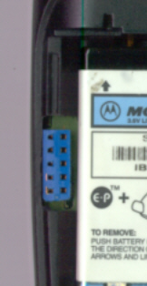 |
I use the same unit as my everyday phone and to experiment on. It's really irritating to continually open, solder, desolder and put the unit back together. Therefore I use a small female 5x2 header that I have soldered directly onto the PCB of my cd930. After trimming the back cover a bit with a file, it sits there just perfectly and there is even room for the battery. An edge of the header had to be rounded so that the battery lid can fit perfectly. I might add another header for the SIM contacts, just to make working with MEDITX easier. |
� 1998 Janus Christian Krarup, Stephan Zegherd & Madis Lobjakas.